 Chinese Researchers Make Breakthrough in Reducing Chip Manufacturing Defects
(Yicai) Oct. 28 -- A research team led by Peng Hailin, a professor at Peking University's College of Chemistry and Molecular Engineering, has managed to reduce pattern defects in chip lithography by using cryo-electron tomography, a method normally used in structural biology.
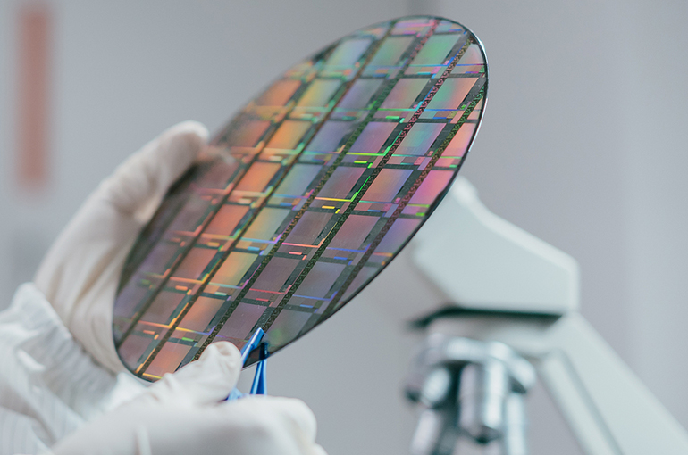
The team used cryo-ET to reconstruct polymer in a liquid film for fab-compatible lithography, reducing the polymer residues of developed patterns on 12-inch wafers by 99 percent, according to findings published in scientific journal Nature on Sept. 30.
Lithography is a key process in semiconductor manufacturing that uses light irradiation to change the solubility of photoresist and then uses developer to dissolve the exposed photoresist to create designed circuit patterns on a silicon wafer.
The new method can be immediately applied in semiconductor manufacturing due to the technology being compatible with existing equipment, Peng told Yicai. Feedback from the industry is necessary for further improvements and for the team to find future study directions, he pointed out.
Liquid film serves as the critical medium for the dissolution of photoresist to create nanoscale circuit patterns in lithography, the team said in the study. However, the microscopic behaviors of photoresist in liquid film and at interfaces remain elusive despite decades of research, leading to industrial effort for pattern defect control being largely a trial-and-error, they noted, adding that the main bottleneck is the absence of a suitable high-resolution imaging technique.
To address this challenge, the team developed the cryo-ET method to reveal the photoresist behaviors in liquid films. Compared with conventional methods, such analysis can reconstruct the three-dimensional structures and interfacial distributions of photoresist polymers at high resolution while maintaining the native structures of polymer-based photoresist in liquid films during imaging and resolving polymer entanglements of photoresist molecules.
The global semiconductor photoresist market topped USD2.7 billion last year and will likely reach USD4.5 billion by 2031, according to QY Research. Leading companies are primarily based in Japan, the United States, and South Korea, including Tokyo Ohka Kogyo, JSR, and Shin-Etsu Chemical, while Chinese firms have broken into the sector with mid to low-end products.
Although China faces restrictions on importing advanced lithography machines, it is still necessary for domestic companies to develop high-end products such as extreme ultraviolet photoresist to catch up with international peers, Peng noted.
Editors: Dou Shicong, Martin Kadiev